domingo, 17 de agosto de 2014

Digital Snake Wing (Part 1) - PLL Test

As you may or may not know, I'm currently working on a Papilio Wing that streams and receives multiple channels of audio over Ethernet using the 5 layer TCP/IP model. The wing includes as an ADC a PCM1807 with a companion PLL1705 to generate the sampling clock frequencies. As a DAC it uses a MAX5556 and as the ethernet controller the ENC28J60.

Here is a render of the PCB and the actual PCB


By the way... I manufactured my PCBs with Elecrow and I have to say I am impressed with their quality. They are really cheap and really good :D.


Anyway... I've just received my Papilio and I'll be posting stuff as I progress.

The first thing I did was to be shure that the PLL was working, so I made a little test module in VHDL that turned on and off a couple of LEDs synchronously with the PLL output clock. Here is the code. Note tha it uses an IP module from Xilinx called DCM. This module is like a programmable PLL and is the one that converts the input 32MHz clock to the 27MHz clock for the PLL1805. You can get more info here http://papilio.cc/index.php?n=Papilio.DigitalClockManager


library IEEE;
use IEEE.STD_LOGIC_1164.ALL;

entity Test_PLL is
    port(
        CK32 : in STD_LOGIC; -- Main Papilio Clock (32MHz)
        CK27 : out STD_LOGIC; -- Clock from the Papilio to the PLL
        CK384fs : in STD_LOGIC; -- Clock from the PLL to the Papilio
        LED1 : out STD_LOGIC;
        LED2 : out STD_LOGIC;
        BTN1 : in STD_LOGIC;
        BTN2 : in STD_LOGIC
        );
end Test_PLL;

architecture Behavioral of Test_PLL is

    COMPONENT DCM32to27
    PORT(
        CLKIN_IN : IN std_logic;          
        CLKFX_OUT : OUT std_logic;
        CLKIN_IBUFG_OUT : OUT std_logic;
        CLK0_OUT : OUT std_logic
        );
    END COMPONENT;
    
signal led1_signal : STD_LOGIC := '0';
signal led2_signal : STD_LOGIC := '1';
begin

    Inst_DCM32to27: DCM32to27 PORT MAP(
        CLKIN_IN => CK32,
        CLKFX_OUT => CK27,
        CLKIN_IBUFG_OUT => open,
        CLK0_OUT => open
    );
    
    -- This process reacts to one of the output clocks of the PLL
    blink: PROCESS(CK384fs)
        variable counter : INTEGER := 0;
    BEGIN
        IF(rising_edge(CK384fs)) THEN
            IF(BTN1 = '1' and BTN2 = '0') THEN -- Button 1 pressed
                counter := counter + 1;
                IF(counter >= 1700000) THEN
                    led1_signal <= not(led1_signal);
                    led2_signal <= not(led2_signal);
                    counter := 0;
                END IF;
            ELSIF(BTN1 = '0' and BTN2 = '1') THEN -- Button 2 pressed
                counter := counter + 1;
                IF(counter >= 17000000) THEN
                    led1_signal <= not(led1_signal);
                    led2_signal <= not(led2_signal);
                    counter := 0;
                END IF;        
            END IF;
        END IF;
    END PROCESS;

    LED1 <= led1_signal;
    LED2 <= led2_signal;    

end Behavioral;

You can also download the Xilinx project from my Github https://github.com/DiegoRosales/VHDL_Modules.git.


lunes, 7 de julio de 2014

DAC Wing for the Papilio Platform

Hello again! This time I decided I would start to share my designs over here as well. This time I'll be sharing a Papilio Wing.
As you may or may not know, the Papilio platform is an awesome barebones FPGA platform with Arduino-style headers to plug what they call "Wings" (instead of shields). Since an FPGA usually has a ton of I/O, you can plug a huge ammount of wings to it (or one Mega Wing) like this.


Since the papilio platform is relatively new, there are not a lot of wings for it. This is why I decided to make a proper audio DAC Wing (they have one, but it's based on PWM and a low-pass filter). The wing I made is EXTREMELY simplistic. It's based on the MAX5556 DAC which barely requires anything. It has only a couple of passives and a 3.5mm stereo jack. This is the render of the board.

kJt2oOE.png

The link for the design files (it is open source, obviously) are here (GitHub)
And here is the link to order the board from OSHPark (It is the prototype version).

jueves, 20 de febrero de 2014

Hercules Launchpad #8 - Nokia 5110 LCD Display (Part 3 - CCS Setup)

Ok, now that we've configured the files in HALcoGen, we have to import the Nokia Libraries. To make this, follow the steps...

Step 1
Create a new project just like we've done it before.

Step 2
Copy the .h and .c files to their respective folders inside the project (include and source, respectively)
OR 
Right-click on the root folder inside CCS and select "Add files...". Then select the library files you downloaded like this


Step 3
Now right-click again on the root folder inside CCS, but this time go to "Properties". Then go to "Include options" and add the directory where you stored the library files.


That's it! When you make use of the libraries you won't have any compiling errors. On Part 4 I'll explain the functions of the libraries...

miércoles, 19 de febrero de 2014

Hercules Launchpad #7 - Nokia 5110 LCD Display (Part 2 - HALcoGen configuration)

So we continue....


Ok, now I feel confident enough to share my progress on the Nokia Display Library.
First I'm going to show you how to configure HALcoGen so that you can use the library.

Step 1
Create a new project just like before...

Step 2
Enable the RTI, GIO, SPI1 and HET drivers.


Step 3
Configure the RTI compare 0 timer to any small value (RTI -> RTI1 Compare). Also enable the interrupt for the compare 0 (RM42L432PZ -> VIM Channel 0-31). This is to generate delays.


Step 4
Configure the HET Drivers. You have to set pin 0 to be a PWM signal and enable the outputs of HET pins 0, 2, 4 and 6.


Step 5
Generate the code! (F5)

Ok, so this is the configuration you will need to be able to use the library. I will leave you with the links of my GitHub so that you can download the library and a demo.
On the part 3 of this tutorial I will explain all the functions I've created.

GitHub

https://github.com/DiegoRosales/Nokia-5110-for-Hercules-Launchpad

domingo, 26 de enero de 2014

Hercules Launchpad #6 - Nokia 5110 LCD Display (Part 1 - The basics)

Esto va a estar bueno...
Pues después de como un mes de pedirlos por eBay, finalmente me llegó mi paquete con 5 displays LCD


y pues, como cualquier persona con el 100% de sus facultades mentales, me puse inmediatamente a ver qué onda con estos displays. Me costó un poco echarlos a andar con el Hercules Launchpad, pero finalmente lo logré y les enseñaré cómo


Pero antes de empezar...
Este tema es muy popular, sin embargo casi toda la información y los recursos que existen (librerías, tutoriales, etc.) están hechos para el Arduino. Es por esto que para que esta información esté disponible para más gente, la explicación será en inglés.

Let's get started!

Ok, so first things first...
Pinouts!!
It is really important to know the pinout of the LCD, as it may vary. The one I got from eBay goes like this
  1. !Reset (RST)
  2. !Chip Enable (CE)
  3. Data / !Command (DC)
  4. Data In / MOSI (DIN)
  5. Clock signal (CLK)
  6. Main source input (Vcc)
  7. Backlight voltage (LIGHT)
  8. Ground (GND)
Another important thing to know is the function of the pins.

!Reset
This is pretty much self explanatory... sort of. This pin resets the microcontroller inside the display to a default state. It is important to know that it is Active Low, meaning that the reset function is triggered when the pin has 0V. Therefore we must maintain this pin on High (3.3V) pretty much all the time.

!Chip Enable
There is not much science about this pin. Whenever you want to tell something to the display, you must activate this pin. This pin is also Active Low, so whenever you try to send something to the display, you must set 0V to this pin.

Data / !Command
This is interesting. There are two kinds of information you can send to the display. The first one is display data. This is the information about what pixels are on and off. The other type of information are commands. This commands are made to achieve several functions such as setting up the contrast levels, inverting the image, setting the cursors, etc. If we want to send display data, we must set a HIGH (3.3V) on this pin. If we want to send a command, we must set a LOW (0V). Pretty straight forward, right?

Data in / MOSI
Ok, so this is the pin where we send the actual information to the display. This display communicates over an SPI (Serial Peripheral Interface) form factor, that's why  we can say it is a MOSI pin (Master Output Slave Input). The Maximum Bit Rate supported by this display is 4Mbits/sec, just remember that. We will discuss the data format later on...

Clock input
There is not much to this. It is part of the SPI protocol. Keep in mind that the maximum clock frequency is given by the maximum bit rate, which is 4Mbits/sec. Therefore, the maximum clock frequency is 4MHz.

Main source input
You must apply 3.3V to this pin. That's it! It doesn't take up much current...

Backlight voltage
This pin is connected to the four LEDs on the board. If you want to see what you're doing in the dark, apply voltage to this pin at will... just be careful, as this boards do not come with current limiting resistors, so they can be very power hungry.

Ground
It is a good practice to connect this pin to Ground... just saying.

Ok... now that you are an expert on the pins of the display, let's see how does it actually work.
The very first thing to do is to reset the display... at least according to the datasheet, see?


According to the datasheet, the reset pulse can be low even before we power up the display, but the time between the power up and the reset pulse must not exceed 30ms. The pulse width of the reset signal must be at least 100ns, which is low enough for us to not worry.
The second thing to do whith it is to initialize the display. This is achieved by sending a series of commands that set up the contrast and other various things. We will see the details of that in the code.
Finally, the last thing to do is to start sending display data.

Now let's discuss the data format.
As I said before, the display controller operates with an SPI interface. This means that it requires a Chip Enable (CE), a Clock Signal (CLK) and one or two data signals (MISO, MOSI). Since this display does not return any data, we only have to worry about one data signal (MOSI).
Another important thing is that the data is sent to the display in packets of 8 bits, with the most significant bit (MSB) first.
The way it is transmitted is the following:


In this case, SDIN is the equivalent of MOSI, SCLK is the Clock signal and SCE is the Chip Enable signal. D/C is the signal that indicates whether we are sending data or commands.
If we want to send several bytes, we just need to keep the SCE low and the clock signal going.
Also, as you can see, each bit is sent in one clock cycle. Not two, not three but one!

Now... let's talk about how the data is displayed on the screen. The micro controller inside the screen has an internal RAM to which we send the display data. This RAM is divided in blocks of 8 bits forming the rows. Therefore it has only 6 rows. It looks like this


Each bit corresponds to a pixel, but we can only manipulate individual bytes, not bits. If we wanted to manipulate a single bit, we would need to have a buffer inside our controller and modify the individual bit there, and then re-send the byte that holds our bit, or just re-send the entire display.

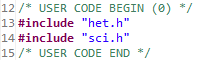
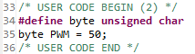
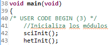
Ok, so pretty much this is what you need to know before you start making your own code!

But before we get into the code, let me tell you a couple of things about the Hercules Launchpad. 
First... it has 3 dedicated SPI modules and one kind of weird Multi-Buffer SPI (MIBSPI). Unfortunately, the MIBSPI/SPI1 pins are the only SPI pins that are soldered. The other 2 modules are in the unsoldered part, and since I didn't want to mess with the MIBSPI/SPI1 module right now, I decided to make the transmitter by software (which isn't hard at all).


************ UPDATE!!! 19/02/2014************

So I decided to stop being lazy and getting into the dedicated SPI ports. As I mentioned, the microcontroller has 3 SPI modules, one of them being a MIBSPI/SPI, which means Multi-Buffer SPI combined with a normal SPI for compatibility. At first I could not make the display ports with it, but after a little investigation and experimentation I made it work.


Second... this is the pin layout of the Launchpad


The connection I made with the display was the following

  • !Reset (RST) ---> N2HET[14]
  • !Chip Enable (CE)  ---> N2HET[12]
  • !Chip Enable (CE)  ---> MIBSPI1nCS1 or GIOA[6] for compatibility with standard boosterpack pinout.
  • Data/!Command (DC) ---> N2HET[10]
  • Data IN (DIN) ---> N2HET[6]
  • Data IN (DIN) ---> MIBSPI1SIMO/ADVERT
  • Clock signal ---> N2HET[4]  
  • Clock signal ---> MIBSPI1CLK
  • Vcc (VCC) ---> N2HET[2]
  • LEDs (LIGHT) ---> N2HET[0]
  • Ground (GND) ---> GND

Note that Vcc is not connected to the 3.3V reference voltage of the launchpad, but instead of a HET pin. This is because this way we have more control over the powerup of the display.


To be continued...


My Github
https://github.com/DiegoRosales

Datasheet

https://www.sparkfun.com/datasheets/LCD/Monochrome/Nokia5110.pdf

Useful videos

http://www.youtube.com/watch?v=M9XBFomX7JI
http://www.youtube.com/watch?v=RAlZ1DHw03g

My Github
https://github.com/DiegoRosales

lunes, 6 de enero de 2014

Hercules Launchpad #5 - Comunicación Serial (SCI / Serial Communications Interface)

Ahora les voy a enseñar cómo hacer que la tarjeta se comunique de manera serial a través del puerto USB para transmitir mensajes.
Como ustedes podrán ver, la tarjeta posee un chip de la marca FTDI. Esta empresa es ampliamente conocida por fabricar circuitos integrados capaces de encargarse de la comunicación serial a través del puerto USB. Este chip en particular es el modelo FT2232HL, que convierte el protocolo USB a UART (Universal Asynchronous Receiver/Transmitter). El protocolo UART es muy sencillo y flexible. Consiste en un bit de inicio, varios bits de datos (este número de bits es predefinido) y uno o dos bits de paro. También puede tener bits de paridad y demás monerías. Como podrán ver en la hoja de datos, este chip tiene muchísimas aplicaciones


En esta tarjeta el chip se usa para dos cosas: 
  • Programación y depuración del procesador a través de la emulación JTAG
  • Comunicación serial usando los protocolos UART
Ahora vamos a hacer un ejemplo donde desde la computadora le mandemos instrucciones al procesador para que cambie el ciclo de trabajo de el LED conectado al puerto HET. Para este ejemplo vamos a utilizar un programa de comunicación serial llamado RealTerm (les dejo el link http://realterm.sourceforge.net/) Comencemos!

Paso 1: Configuración en HALcoGen
Lo primero que hay que hacer es configurar la tarjeta en HALcoGen.

Paso 1.1: Driver Enable
En la pestaña que dice "Driver Enable", habilitamos las casillas que dicen "Enable SCI Driver" y "Enable HET Drivers".

Paso 1.2: HET
Ahora vamos a configurar el HET para que se inicialice con un ciclo de trabajo del 50% a una frecuencia de 1Hz.
Para esto, en la subpestaña que dice "PWM 0-7" nos vamos al primer PWM y lo configuramos para que posea un periodo de 1000000us y un ciclo de trabajo del 50% y lo habilitamos para que salga al pin 8.


Luego, en la subpestaña que dice "Pin 8-15", habilitamos el pin 8 para que sea salida.


Paso 1.3: SCI
Ahora vamos a configurar el SCI. Para esto nos vamos a la pestaña que dice "SCI" y en la subpestaña que dice "SCI/LIN Data Format" hacemos que esté a una frecuencia (baudrate) de 9600 con 2 bits de paro, 8 bits de datos y sin bits de paridad.


Ya tenemos todo listo. Ahora hay que generar el código (F5).

Paso 2: Escribir el Programa
Como se podrán imaginar, el módulo SCI posee varias funciones para poder ser utilizado con facilidad. A continuación veremos cuáles vamos a usar.

Paso 2.1: Configurar el proyecto en Code Composer Studio
Ahora abrimos Code Composer Studio y lo configuramos como lo hemos hecho siempre

Paso 2.2: Escribir el programa principal
Abrimos el archivo que dice "sys_main.c" y escribimos lo siguiente.
Primero hay que incluir todo lo que necesitamos. Esto es, los headers de el SCI y del HET


Luego, para facilitar el programa, hay que definir un tipo usando #define. El tipo que hay que definir es "unsigned char", que es una variable de 8 bits ("char") sin signo ni nada ("unsigned"). A este tipo le vamos a llamar "byte". Esto se hace así.


Pueden ver que también definí una variable llamada "PWM" tipo "byte". Esta va a ser la variable que va a almacenar el ciclo de trabajo que le vamos a mandar desde la computadora.
Ahora hay que inicializar los módulos


Ahora viene lo bueno. En el manual de HALcoGen, en la sección del SCI, pueden ver que hay una función llamada "sciReceive" y nos da la siguiente explicación.


Lo que esta función hace es esperar a que le mandemos un dato de 8 bits con 2 bits de paro y ningún bit de paridad (como lo definimos en HALcoGen). Esta función detiene el flujo del programa hasta que no reciba el dato. Sin embargo, el LED no va a dejar de parpadear por eso, ya que el HET funciona de manera independiente al flujo del programa.
Lo que hay que introducir a esta función para que haga su trabajo es la dirección del módulo, la cantidad de "bytes" que va a recibir (en este caso sólo es 1) y un apuntador diciendo dónde vamos a guardar el dato recibido.

Nota 1: la cantidad de los bytes que vamos a recibir debe ser igual al tamaño de la variable en la que los vamos a guardar. En este caso el tamaño es 1, pero puede ser un arreglo indefinido de bytes (por ejemplo "byte variable[] = "Hola Mundo!""), por lo que hay que usar funciones como "sizeof()" para determinar el número de bytes que vamos a recibir. De otro modo, vamos a tener errores que el compilador no va a detectar.

Continuemos...

El código resultante de esto queda de la siguiente manera.


Pueden ver que agregue una sección donde checa si el PWM ingresado es válido o no.

Paso 3: Probar la comunicación
Existen varias maneras de establecer una comunicación serial en la computadora. Una es utilizando la terminal serial que trae Code Composer Studio. Sin embargo, yo les voy a mostrar un programa llamado RealTerm que está muy completo y tiene un chorro de monerías.

Paso 3.1: abrir RealTerm
Abrimos RealTerm y nos aparece la siguiente pantalla.


En esta pestaña (Display) nos aseguramos que esté seleccionado Ascii (aunque la verdad no me he puesto a ver si funciona igual con los demás).

Paso 3.2: Configurar el puerto
Ahora nos vamos a la pestaña que dice "Port" y hacemos los siguientes ajustes: Parity None, Data Bits 8, Stop Bits 2, Baud 9600, Port 4 (o donde esté conectado la tarjeta. Esto se puede ver en el administrador de dispositivos en la categoría de puertos COM y LPT). Ya que tenemos todo como se muestra, le damos clic en "Change" y luego en "Open".


Paso 3.3 Mandar datos
Ahora nos vamos a la pestaña que dice "Send" y ya podemos comenzar a mandarle datos. En la casilla de texto escribimos un número y luego le damos clic en "Send Numbers".


Así de sencillo fue!

Nota 2: La funcion "sciSend" es igual de fácil de utilizar que el "sciReceive" y funciona perfectamente con RealTerm.

Luego les enseñaré cómo hacer un programa en Visual Studio que se comunique a través del puerto serial.

Les dejo el link del código


My Github
https://github.com/DiegoRosales